How to Reverse Engineer PCB for Success at 2026 Canton Fair?
The upcoming 2026 Canton Fair presents a prime opportunity for businesses aiming for success in the electronics sector. Reverse Engineering Pcb can unlock significant advantages in understanding the latest technologies and market trends. With an emphasis on advanced manufacturing and electronic appliances, this fair will witness an influx of innovators and suppliers.
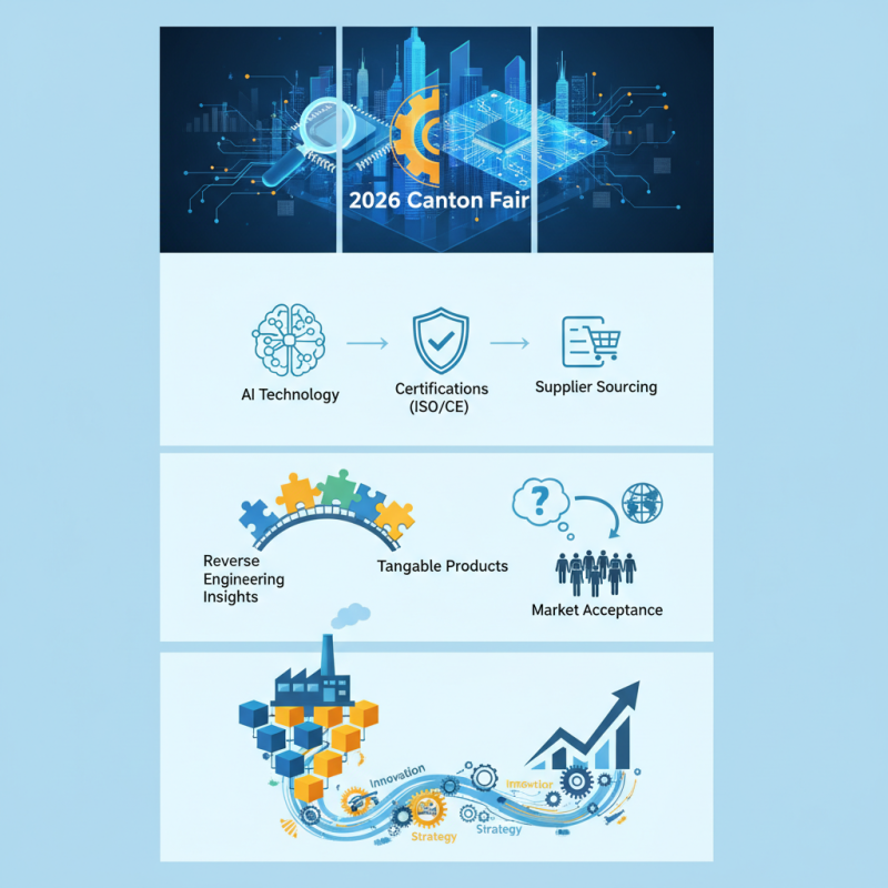
The integration of AI technology at the fair elevates the importance of efficient navigation and supplier sourcing. It allows buyers to quickly identify relevant vendors. For instance, finding suppliers with ISO or CE certifications can streamline acquisition processes. Yet, the challenge remains in the precise application of knowledge gained through reverse engineering PCB. Have businesses fully assessed their capacity to adapt to the rapid changes in tech?
Moreover, while the fair is a platform, there are underlying complexities. How well can one translate the insights from reverse engineering into tangible products? What about the unforeseen challenges in market acceptance? Companies must reflect on their strategies to leverage the insights gleaned from the event effectively. Building a strong foundation is essential for long-term success in the competitive landscape.
Understanding the Basics of PCB Design and Functionality
Reverse engineering a printed circuit board (PCB) requires a solid understanding of PCB design and functionality. Many experts in the electronics industry agree that recognizing the basic principles is crucial to success. A recent report by Technavio states that the global PCB market is expected to grow by over 4% annually, emphasizing the increasing importance of effective PCB design. Proper design can improve not only performance but also cost-effectiveness.
Designing a PCB involves laying out circuits that ensure proper electrical connectivity. This requires knowledge of components, such as resistors and capacitors, and how they interact. At the same time, understanding the manufacturing process is critical. Designing for manufacturability is often overlooked. Mistakes here can lead to increased production costs and delays. A focus on durability and heat dissipation can prevent future issues.
Stepping into the world of PCB design can be daunting. Many find themselves grappling with complex software and intricate layouts. Moreover, common pitfalls include poor routing practices and signal integrity issues. Reflecting on these challenges can lead to better strategies for future projects. Emphasis on iterative testing and validation can ultimately enhance the success rate at the 2026 Canton Fair.
Essential Tools and Software for PCB Reverse Engineering
Reverse engineering a PCB can seem daunting. Yet, with the right tools and software, you can simplify the process. A good starting point is a high-resolution camera or microscope. This will help you capture the details of the board. Pay attention to the traces and components. Small details can make a big difference.
For software, consider using tools for schematic capture. These will allow you to replicate the circuit more effectively. In addition, PCB design software can help you recreate the layout. Always test your designs thoroughly. Sometimes, minor errors can lead to major issues later on.
**Tips:** Keep backups of your designs. Mistakes happen, and it's best to have a fallback option. Also, document your process. It will help you track improvements and reflect on past challenges. Stay organized, and remember that patience is key. Each setback is a learning opportunity.
Step-by-Step Process of Reverse Engineering a PCB
Reverse engineering a printed circuit board (PCB) can be a complex yet rewarding endeavor. To effectively reverse engineer a PCB for success at the 2026 Canton Fair, a structured approach is vital. Start by obtaining the PCB and carefully examining its components. You might need tools like a microscope and a multimeter to identify various parts. Industry reports indicate that about 70% of new electronic products use similar components. This means analyzing common components can save time.
Documenting every step is crucial. Use detailed annotations to note findings on the circuit design. Identifying traces can boost understanding of the PCB’s functionality. A study from the Electronics Manufacturing Association shows that 65% of engineers reported improved productivity through comprehensive documentation. Despite this, shortcomings often arise. Some engineers miss vital connections or misinterpret component roles, which may lead to flaws in the final design.
Testing is another essential step. After reverse engineering, prototype your findings. It’s not always straightforward. Many prototypes fail or work differently than expected. Understanding that failure is part of the process aids in refining your approach. Accurate reverse engineering demands patience and iteration. Continued practice will enhance your skills and prepare you for showcasing innovative ideas at international events like the Canton Fair.
Common Challenges in PCB Reverse Engineering and Solutions
Reverse engineering PCBs can be challenging, especially for newcomers. One major hurdle is understanding the circuit design. It's not just about copying a layout; recognizing how each component interacts is crucial. This step can seem daunting. Not every design is straightforward. Some may even have hidden elements that complicate the process.
Another common issue is sourcing the right materials. Finding exact matches for components isn't always possible. Alternative parts might not perform identically. Testing is essential here. Sometimes, the initial tests reveal flaws. It’s vital to adjust and iterate, learning from each attempt. Each failure can offer valuable insights.
Documentation plays a significant role in reverse engineering. Many overlook the need for meticulous notes. A lack of clear records can lead to confusion later. It's easy to forget details in complex projects. Creating a comprehensive guide helps keep track of changes and findings. Remember, refining the process is key to eventually mastering PCB reverse engineering.
Utilizing Reverse Engineered PCBs to Enhance Product Development
Reverse engineering printed circuit boards (PCBs) can significantly boost product development. This method allows firms to analyze competitors' designs and enhance their own offerings. By understanding the intricacies of a PCB, manufacturers can innovate and create better products.
When reverse engineering, focus on functionality. Disassemble competitors’ PCBs carefully. Identify components and their specifications. Document your findings in detail. This documentation will help guide your own design process. Errors and inconsistencies are learning opportunities. Reflect on what works and what doesn’t.
Tips: Look for common patterns in successful designs. Experiment with variations based on your research. Testing is key. Use prototypes to evaluate designs quickly.
Another crucial aspect is collaboration. Engage team members in discussions about your findings. Different perspectives can lead to innovative solutions. Brainstorm improvements. Constructive feedback is essential. Use it to refine your approach and enhance outcomes. Embrace imperfection; it’s part of the journey toward success.